For a long time, my digital setup on VHF was as simple as it gets. At the heart of my station is a trusty Yaesu FT-897 all-mode transceiver. I had a generic Chinese CAT cable built around an FTDI chip, and a DIY audio interface that I threw together using two small isolation transformers tucked into a plastic wall-wart power adapter shell. In that same plastic casing, I crammed an isolated FTDI module that handled hardware PTT keying for both the FT-897 and an external amplifier.
As long as I ran "barefoot" straight out of the FT-897 — around 50 watts on 144 MHz — everything worked like a charm. WSJT-X decoded weak FT8 and MSK144 signals without a hitch, CAT commands never dropped, and contacts went smoothly into the log.
Then, curiosity took over. I got my hands on three different Russian tube power amplifiers to test out in the shack:
- A single GI-7B (ГИ-7б) triode amplifier putting out around 200 W.
- A GI-46B (ГИ-46б) amplifier delivering a solid 500 W.
- A heavy-duty GS-35B (ГС-35б) amplifier capable of 700+ W, which yielded around 500 W on my bench because my transceiver could only deliver 50 W of drive.
That was the exact moment my peaceful digital operation came to a screeching halt.
The audio path through the transformers was actually holding up fine — the real crisis was strictly the digital control lines. The second I keyed up with any of these amplifiers in line, the PTT line would trip almost instantly, dropping the transceiver right back into receive mode mid-transmission. The intense VHF RF field was crashing the FTDI chip in my PTT box — it would lock up or reboot, completely disappearing from the computer's Device Manager. Seconds later, the Chinese CAT cable would follow suit: its own FTDI chip would reset, severing rig control and leaving WSJT-X frozen with a communication timeout error.
The culprit was obvious: unshielded plastic enclosures, bare cables acting as antennas, and a total lack of RF common-mode filtration. At 50 watts you can get away with plastic project boxes and loose wiring. At 200 to 500 watts of VHF RF, common-mode currents will find every crack in your setup and wreck havoc on high-speed digital electronics.
Patching the existing mess with snap-on ferrite beads helped a tiny bit, but it was just a band-aid. I needed a permanent, clean, all-in-one solution. And since I was going to design a custom PCB from the ground up anyway, I decided to do it right from top to bottom: house it in a rugged, fully shielded aluminum enclosure, clamp down RF at every single I/O port, use 100% galvanic isolation, and treat the audio path to high-grade permalloy transformers with onboard gain trimmers.
A quick hobbyist disclaimer: Before we look at the circuit, let me be very clear — I am not a professional electrical engineer or a professional PCB designer. Electronics and amateur radio are strictly my personal hobby. I design these boards at home to solve real problems on my own workbench, learning as I go. While this interface completely solved my RF tripping issues and works reliably in my station, there are almost certainly design quirks, suboptimal component choices, or subtle oversights in the schematic and layout. Please treat this project as one hobbyist sharing his notes with the community rather than an industrial standard. If you spot mistakes or have ideas for improvement, I always welcome feedback from fellow builders!
The Ground Architecture: Three Isolated Ground Domains
If your computer and your transceiver share even a single millivolt of common ground potential over copper, you have already lost the battle. But there is a crucial architectural nuance here that many simple interfaces overlook: in this device, there are actually three separate ground domains on the board:
- The PC Digital Ground (
GND_NOISELESS): Powered strictly by the computer's +5V USB bus, referencing the FTDI FT232RL USB-to-UART bridge and the primary (PC) side of the optocouplers. - The PC Soundcard Audio Ground (
GND): Connected exclusively to the 3.5 mm stereo audio cable shield running to the computer's sound card Line In and Line Out. - The Radio Analog Ground (
GND_ANALOG): Referenced to the Yaesu FT-897's chassis via the CAT and DATA connectors, powering the radio-side optocoupler stages and the 78L05 linear regulator.
Why keep GND and GND_NOISELESS strictly separate inside the interface?
Inside your PC motherboard, the soundcard analog ground and the USB digital ground are already connected to a shared chassis plane. A builder might naturally ask: \"Why not just bridge them on the interface PCB as well?\" Doing so is one of the most common pitfalls in shack audio design! If you connect them at the interface end, you create a closed ground loop running between the PC, down the USB cable shield, through the interface PCB, and back up the audio cable shield to the sound card. Any stray 50/60 Hz magnetic fields or localized VHF RF picked up along those cables will circulate common-mode current through that copper loop, directly modulating the audio line and injecting hum, buzz, or RF hash into your WSJT-X waterfall. By keeping GND and GND_NOISELESS completely floating with respect to each other on the PCB, the computer remains the single star-ground reference — zero circulating loop currents.
And between both PC-side grounds and the radio side (GND_ANALOG), there is zero DC connection whatsoever. Every single signal crosses either via photons (6N137 and PC817 optocouplers) or magnetic flux (E-9818 permalloy audio transformers).
Deep Dive into the Schematic
Let’s trace the circuit section by section, from the USB plug to the radio accessory socket.
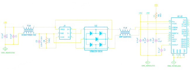
1. Hardening the USB Ingress (J1, U1 & U2)
When high RF fields hit an external USB cable, aggressive common-mode currents try to travel down the copper and dump into the computer's motherboard or reset the USB bridge. To prevent this, the input stage at connector J1 uses a strict multi-layer defense:
- The Shield Snubber (C3 + R8): Rather than hard-grounding the USB connector metal shield (
J1) directly to the board's internal digital plane, it is terminated to the incoming cable's rawGNDpin (at connector J1, before common-mode chokeFL8) through a parallel network of high-voltage ceramic capacitor C3 (2.2 nF, 2 kV) and bleeder resistor R8 (1 MΩ, SMD 0805). This drains ESD and shunts high-frequency shield currents directly back into the cable sheath without letting common-mode RF enter the internalGND_NOISELESSplane, breaking the antenna ground loop. Because virtually zero continuous DC current flows through 1 MΩ, a compact 0805 SMD resistor is ideal and saves board space. - First Line of Defense on Data: ESD Clamping (U2 / USBLC6-2SC6): The D+ and D- lines from J1 immediately hit U2, a dedicated high-speed ESD protection diode array with ultra-low sub-picofarad parasitic capacitance. Placing U2 directly adjacent to the connector pins clamps high-voltage static discharges before they can penetrate deeper into the board.
- Data Common-Mode Choke (FL9 / SRF3225TAC): Directly after the ESD diodes, the D+ and D- differential pair passes through a specialized SMD common-mode choke FL9 (Bourns SRF3225TAC). It is completely transparent to the USB differential data signals, but acts as a massive barrier against high-frequency common-mode VHF/UHF currents induced by external RF fields.
- USB Power Filtration (FL8 / SCM474520): The incoming +5V VBUS and its ground return pass through heavy-duty common-mode choke FL8 (SCM474520), followed by a π-filter with bypass capacitors C1 (10 µF) and C2 (0.1 µF). This eliminates high-frequency noise and switching hash from both the PC bus and external RF pickup.
- The USB-to-UART Bridge (U1 / FTDI FT232RL): Only after power and data lines have been thoroughly clamped and filtered do they reach U1 (FTDI FT232RL). Operating in an RF-quiet zone on the
GND_NOISELESSplane, U1 handles the USB-to-UART protocol conversion reliably and provides our hardware control lines (DTR#,TXD,RXD) without crashing or dropping off the bus.
2. High-Speed CAT Isolation (VO1 & VO2 / 6N137)
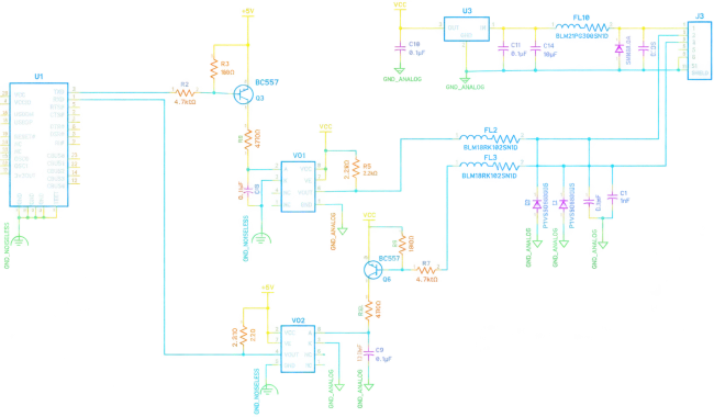
The Yaesu FT-897's CAT interface operates on standard TTL voltage levels (0–5V) directly on its 8-pin mini-DIN port (J3) — no legacy RS-232 level-shifting ICs (like MAX232) are required. However, slow general-purpose optocouplers like the ubiquitous PC817 are far too sluggish for serial data, rounding off the edges of 4800, 9600, or 38400 baud serial pulses into useless mush.
- For the serial data lines, I used 6N137 high-speed optocouplers (
VO1andVO2), which easily handle data rates up to 10 MBaud with active logic output stages and integrated Faraday shields for superior common-mode noise rejection. - TXD Path (PC to Radio): The
TXDpin from the FT232RL drives a PNP transistor buffer Q3 (BC557) via base resistor R2 (4.7 kΩ) and pull-up resistor R3 (10 kΩ to +5V). In the UART idle state (Mark / +5V), Q3 remains cutoff. When a start bit or data zero (Space / 0V) arrives, Q3 saturates and sources current through R4 (470 Ω) into the GaAsP infrared LED of VO1. The receiving side of the 6N137 features an active open-collector output pulled up to the radio'sVCC(+5V) via R5 (2.2 kΩ). Because both the PNP driver and the 6N137 open-collector output invert the signal, the two inversions cancel out perfectly — delivering a crisp, non-inverted serial data stream directly to the radio. - TX Output Filtering & Port Protection: From the
VOUTpin of VO1, the signal passes through an L-section (Г-образный) low-pass filter formed by series ferrite bead FL2 (Murata BLM18RK102SN1D, 1000 Ω @ 100 MHz) and shunt ceramic capacitor C17 (1 nF) before reaching pin 2 of connector J3. Right at the connector terminal, a 5V unidirectional TVS diode D12 (PTVS5V0S1UR) clamps electrostatic discharges and induced RF voltage spikes toGND_ANALOG. With a circuit time constant of $\approx 2.2\ \mu\text{s}$, the 1 nF capacitor presents near-zero impedance to 144 MHz VHF currents without degrading UART pulse edges even at 38.4 kBaud. - RXD Path (Radio to PC): The incoming serial stream from the radio arrives on pin 3 of connector J3. It is immediately clamped by TVS diode D4 (PTVS5V0S1UR) and cleaned by a matching filter network (shunt capacitor C18, 1 nF, and series ferrite bead FL3, BLM18RK102SN1D). The signal drives PNP buffer Q6 (BC557) via R7 (4.7 kΩ) and R10 (10 kΩ pull-up to
VCC), keying the LED of VO2 through R8 (470 Ω). On the computer side, VO2’s open-collector output drives the FT232RL’sRXDline, with pull-up resistor R14 (2.2 kΩ) tied to the USB +5V bus. - Radio-Side Power Supply (
VCC): The active circuitry on the transceiver side — specifically the output stage of optocoupler VO1 (pin 8 and pull-up resistor R6) and the bias network for PNP transistor Q6 (emitter and base pull-up resistor R10) — requires clean +5V power referenced strictly toGND_ANALOG. Instead of bridging power from the PC across the isolation barrier, thisVCCrail is tapped directly from the Yaesu FT-897's +13.8V pin on pin 1 of connector J3, heavily filtered against RF, and regulated down to +5V by onboard linear regulator U3 (L78L05).
3. PTT Switching: Transceiver and Aux Keying (Q1, Q5 & K2)
Digital modes require ultra-reliable hardware PTT. Relying solely on software CAT commands (TX; / RX;) over serial is risky — if a serial packet drops or times out during a heavy RF burst, the transceiver can get stuck in transmit mode. Dedicated hardware PTT provides deterministic, instantaneous transmit/receive control.
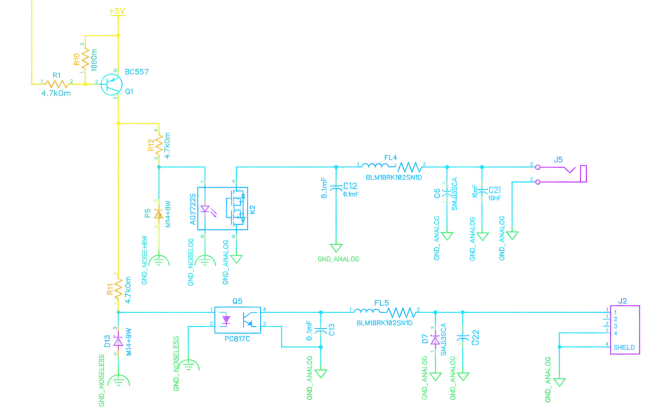
- PTT Control Line (
DTR#& Q1): I selected the FT232RL’sDTR#pin (pin 2) to trigger PTT from WSJT-X. In receive mode,DTR#sits high (+5V), keeping PNP transistor Q1 (BC557) in cutoff. When WSJT-X triggers transmission, it pullsDTR#active-low (0V). This draws base current through resistor R1 (4.7 kΩ) (with pull-up R10 (10 kΩ)), driving Q1 into hard saturation and applying +5V from the USB bus (GND_NOISELESS) to simultaneously key two independent, fully isolated PTT stages:- Amplifier Keying (K2 / AQY212 PhotoMOS Relay): Keying high-power tube amplifiers requires a rugged switch. Traditional optotransistors (like 4N35) have limited current ratings (~50 mA) and can easily fail from back-EMF spikes. I chose the AQY212 PhotoMOS solid-state relay (K2), driven via current-limiting resistor R12 (470 Ω) with anti-parallel diode D5 (1N4148W). Its bi-directional MOSFET output handles continuous currents up to 500 mA and peak loads up to 60V with zero contact bounce — plenty of overhead to safely switch even the most power-hungry 24V vacuum relays (like REV-14/15 or vacuum contactors) without welding or arcing.
Amplifier PTT Filtering & 30V Surge Protection (J5): K2's output connects to rear RCA jack J5 through a heavy-duty RF filtering and clamping network: shunt capacitor C12 (0.1 µF), high-impedance series ferrite bead FL4 (Murata BLM18RK102SN1D, 1000 Ω @ 100 MHz), shunt capacitor C21 (10 nF), and a transient suppressor diode D6 (SMDJ30CA). I specifically selected a bidirectional 30V TVS diode (SMDJ30CA) here because my external tube amplifier switches on a 24V DC relay supply rail. A standard 15V TVS would conduct and blow immediately under 24V operation, whereas the SMDJ30CA sits completely idle during normal 24V switching while instantly clamping destructive inductive kickback spikes when the relay coils de-energize. - Transceiver Keying (Q5 / PC817C Optocoupler): For the radio itself, current flows from Q1 through R11 (470 Ω) and diode D13 (1N4148W) into the LED of Q5 (Sharp PC817C). The isolated phototransistor on the radio side pulls the transceiver’s PTT line down to
GND_ANALOG.
Radio PTT Filtering & 15V Surge Protection (J2): The radio PTT line uses an identical low-pass filter and surge suppression topology: shunt capacitor C13 (0.1 µF), series ferrite bead FL5 (Murata BLM18RK102SN1D), shunt capacitor C22 (10 nF), and transient suppressor D7 (SMDJ15CA), outputting to pin 1 of connector J2 (4-pin mini-DIN DATA port). Because the Yaesu FT-897's internal control circuitry references 13.8V / 5V logic, a 15V TVS (SMDJ15CA) provides the perfect clamping ceiling without nuisance tripping.
- Amplifier Keying (K2 / AQY212 PhotoMOS Relay): Keying high-power tube amplifiers requires a rugged switch. Traditional optotransistors (like 4N35) have limited current ratings (~50 mA) and can easily fail from back-EMF spikes. I chose the AQY212 PhotoMOS solid-state relay (K2), driven via current-limiting resistor R12 (470 Ω) with anti-parallel diode D5 (1N4148W). Its bi-directional MOSFET output handles continuous currents up to 500 mA and peak loads up to 60V with zero contact bounce — plenty of overhead to safely switch even the most power-hungry 24V vacuum relays (like REV-14/15 or vacuum contactors) without welding or arcing.
4. Audio Isolation: The AF Signal Path (T3 & T4 / E-9818)
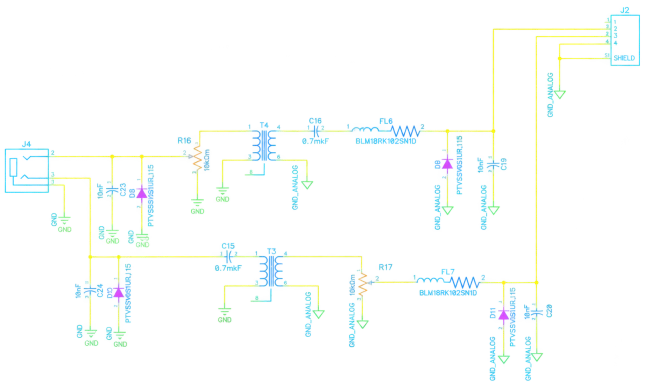
While the audio path in my makeshift setup wasn't causing the dropouts, building a brand-new interface from scratch was the perfect opportunity to do the soundcard interface properly. Rather than reusing mystery junk-box audio transformers, I selected matched E-9818 permalloy-core transformers (1:1 ratio, 600:600 Ω). The high-permeability nickel-iron (permalloy) cores deliver an exceptionally flat frequency response from 20 Hz to 20 kHz with minimal phase distortion across the audio spectrum — ensuring clean, linear audio transfer to and from WSJT-X.
- TX Audio Path (PC Line Out to Radio Data In):
- Audio from the PC sound card enters on pin 3 of 3.5 mm jack J4. The line is immediately filtered by shunt capacitor C24 (10 nF) and clamped against ESD by D10 (PTVS5V0S1UR) to the soundcard ground plane (
GND). - Before reaching the primary winding of transformer T3 (E-9818), the signal passes through series DC-blocking capacitor C15 (0.7 µF). This is critical: consumer sound cards often leak a small DC offset, and even 1–2 mA of continuous DC current through a miniature transformer will bias and saturate the permalloy core, drastically cutting inductance and creating severe harmonic intermodulation (IMD). The 0.7 µF capacitor completely eliminates DC bias current and forms a high-pass pole ($f_c \approx 380\text{ Hz}$ with 600 Ω), effectively passing the active FT8 and weak-signal digital subcarrier band while cleanly rejecting 50/60 Hz AC mains hum and low-frequency rumble.
- On the radio side (
GND_ANALOG), the isolated secondary winding feeds multi-turn potentiometer R17 (10 kΩ), allowing precise analog level trimming before the transceiver's modulator. - From the wiper of R17, the TX audio passes through high-frequency ferrite bead FL7 (Murata BLM18RK102SN1D, 1000 Ω @ 100 MHz), TVS diode D11 (PTVS5V0S1UR), and RF bypass capacitor C20 (10 nF) before outputting on pin 3 of connector J2 (6-pin mini-DIN DATA port) to the transceiver.
- Audio from the PC sound card enters on pin 3 of 3.5 mm jack J4. The line is immediately filtered by shunt capacitor C24 (10 nF) and clamped against ESD by D10 (PTVS5V0S1UR) to the soundcard ground plane (
- RX Audio Path (Radio Data Out to PC Line In):
- Received audio from the transceiver arrives on pin 2 of connector J2. It is immediately filtered and protected against RF by shunt capacitor C19 (10 nF), TVS diode D9 (PTVS5V0S1UR), and series ferrite bead FL6 (Murata BLM18RK102SN1D).
- Series capacitor C16 (0.7 µF) strips away any transceiver DC bias voltage before the signal enters the primary of transformer T4 (E-9818).
- On the soundcard side (
GND), the secondary winding connects to trimmer potentiometer R16 (10 kΩ), which pads down the fixed-level radio audio so the PC's audio input never clips or overloads. - From R16, the signal passes TVS diode D8 (PTVS5V0S1UR) and bypass capacitor C23 (10 nF), exiting on pin 2 of 3.5 mm jack J4 into the computer's sound card Line In / Mic input.
5. Radio-Side Power Supply (U3 / L78L05)
The isolated optocouplers and transistors on the radio side cannot run on magic; they need clean DC power. But pulling that power from the USB bus via a DC-DC converter would defeat the purpose by introducing switching noise and parasitic capacitive coupling across the barrier.
Instead, the interface taps the +13.8V auxiliary power pin provided directly by the Yaesu FT-897's CAT port (pin 1):
- Power enters connector
J3, passes through a beefy SMDJ15CA transient suppressor D3, a high-current ferrite bead FL10 (Murata BLM21PG300SN1D, 0805, 3A), and filter capacitors C25 and C14. - A linear regulator U3 (L78L05) steps this down to a rock-solid +5V (
VCC) referenced strictly toGND_ANALOG, supplying clean DC to the radio-side circuitry including optocoupler VO1 and buffer transistor Q6. Total current consumption is only around 15–25 mA, so the regulator barely gets warm.
PCB Layout: The Engineering That Makes It Work
A schematic is just an intention; the PCB layout is the physical reality. In high-power VHF environments, a sloppy PCB trace will act as an inductor, and adjacent copper pours will act as capacitors, bypassing your isolation entirely.
The PCB is dimensioned at 99.9 × 59.8 mm to slide directly into standard extruded aluminum enclosures (such as the Hammond 1455 series).
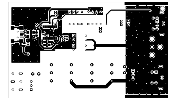
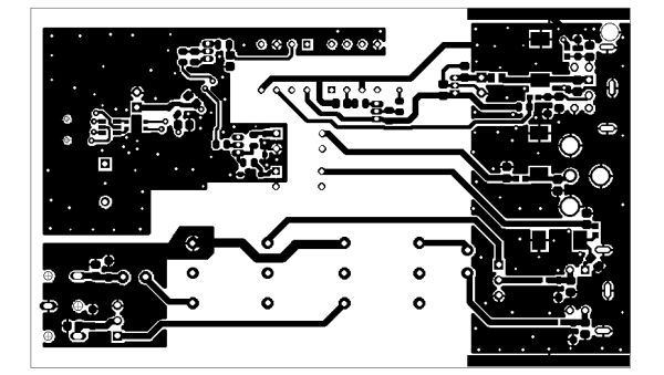
Key Board Layout Decisions:
- The Isolation "Moat": Running right through the board is a complete void in copper. No ground planes, no power traces, and no signal lines cross this 15–20 mm gap. The only bridges across the canyon are the optical paths inside the DIP chips and the magnetic cores of the transformers.
- "Hardened I/O" at the Board Edge: Look closely at the bottom layer of the board near connectors J2, J3, and J5. All the TVS diodes and Murata BLM ferrite beads are placed literally within millimeters of the connector pins. RF energy entering the box hits the shunt TVS and bypass caps immediately, dumping to the enclosure shield before it can travel even half an inch across the board.
- Stitched Ground Flood: The radio-side ground plane is flooded with solid copper on both top and bottom layers, stitched together with dozens of vias. This eliminates parasitic ground loops and keeps the RF impedance as close to zero as physically possible.
- Enclosure Grounding: The entire board slides into a die-cast or extruded aluminum box. The metal chassis is connected to
GND_ANALOGat a single point near the radio connector shells, turning the box into a continuous Faraday cage. It must never touchGND_NOISELESS.
The Assembled Hardware
Here is how the finished build came together on the bench:
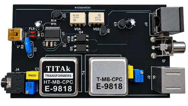
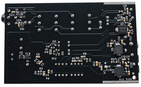
And here is the unit fully assembled into its extruded aluminum enclosure:
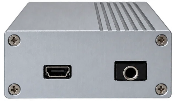
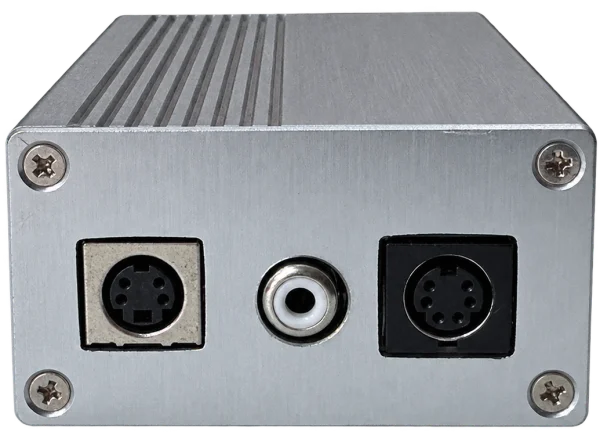
Notice the physical construction and enclosure grounding strategy here, as it plays a massive role in surviving 500 W VHF fields:
- Extruded Aluminum Enclosure: The PCB slides directly into the internal card guides of a heavy-duty extruded aluminum case (Hammond 1455 style). Plastic project boxes are completely transparent to VHF/UHF electric and magnetic fields; a solid metal shell is mandatory to form an unbroken 360-degree Faraday cage around the circuitry.
- Bonded Exclusively to
GND_ANALOG: The aluminum enclosure is electrically bonded at a single physical point to the transceiver ground (GND_ANALOG) right at the rear connector panel (near mini-DIN connectors J2, J3, and RCA jack J5). - Why
GND_ANALOGand NOT the PC ground? A common question is: "Why tie the metal case to the radio ground instead of the computer's USB ground or soundcard ground?"- Extension of the Radio Chassis: The Yaesu FT-897 already has a heavy die-cast metal body tied to the station RF ground and antenna feeder braid. By bonding the interface enclosure to
GND_ANALOG, the aluminum box effectively becomes a seamless physical extension of the transceiver's shielded chassis. - Shunting Common-Mode RF Outside the Circuit: When operating high power (200–500 W) on 2 meters, high-intensity RF fields radiate from the amplifier tank circuit and antenna feedline. Any common-mode VHF currents picked up on the exterior of the interconnect cables meet the aluminum case first. Because the case is tied to
GND_ANALOG, these currents are shunted harmlessly across the exterior metal skin straight back to the radio chassis and station earth, without ever penetrating the interior or circulating through signal traces. - Protecting the PC and FTDI Bridge: If the metal case were tied to
GND_NOISELESS(the PC USB ground) orGND(soundcard ground), the entire aluminum shell would act as an antenna in the near-field of the tube amplifier. It would collect stray VHF RF and dump it directly down the USB cable into the PC motherboard and FT232RL bridge — causing instant USB bus resets, driver crashes, and defeating the entire isolation moat. - Front Panel Isolation: On the front panel, the mini-USB jack (J1) and 3.5 mm audio jack (J4) are kept strictly isolated from the aluminum casing. The USB connector shield connects to
GND_NOISELESSonly through the high-voltage snubber (C3 / R2), and neither PC-side ground plane ever touches the enclosure. This ensures zero circulating DC or RF ground loops between the computer and the interface.
- Extension of the Radio Chassis: The Yaesu FT-897 already has a heavy die-cast metal body tied to the station RF ground and antenna feeder braid. By bonding the interface enclosure to
Custom Interconnect Cables: Why Even the Ground Wire Gets a Shield
A bulletproof, RF-hardened interface is only as good as the cables tethering it to your gear. If you use flimsy unshielded patch cords or cheap unshielded ribbons, those wires act as efficient resonant antennas at 144 MHz, sucking in stray VHF energy from your 500 W amplifier and piping it directly past your enclosure shielding.
To connect the interface to my station, I fabricated custom shielded interconnects for all four ports:
- CAT Cable: 8-pin mini-DIN to connector
J3(TXD, RXD, +13.8V, GND). - DATA Cable: 4-pin mini-DIN (interface J2) to 6-pin mini-DIN (transceiver DATA port) carrying TX audio, RX audio, Transceiver PTT, and GND.
- PC Audio Cable: High-grade shielded cable with 3.5 mm TRS stereo plugs to connector
J4. - Amplifier PTT Cable: Shielded coax/RCA patch lead to connector
J5.
For the multi-pin cables (CAT and DATA), I selected high-quality shielded multi-conductor cable featuring a dense tinned copper braided shield. But rather than following standard consumer cable construction, I used a specific grounding technique:
The Dedicated Internal Ground Conductor
In cheap commercial cables, manufacturers cut corners by using the outer braided shield as the only ground return path. In my custom cables, I allocated a dedicated internal insulated conductor strictly for Ground, and at both ends of the cable (inside the connector shells), I soldered this internal ground wire in parallel with the outer braided shield. In other words, the ground return path itself travels entirely inside the outer shield.
Why go through the extra trouble of shielding the ground wire inside the cable?
- Shield-Current-Induced Noise (SCIN) & Skin Effect: When operating a 500 W amplifier on VHF, the intense electromagnetic field induces high-frequency common-mode RF currents on the exterior of the cable. Due to the skin effect, these high-frequency currents travel exclusively on the outer surface of the braided shield. If that outer shield is your only ground conductor, the RF currents traversing the braid's transfer impedance create a high-frequency voltage drop (\(V = I_{RF} \cdot Z_{shield}\)) directly across the signal return line, superimposing RF hash onto your serial data and audio. By providing an internal insulated ground conductor running through the core, your clean return current flows through a path physically protected inside the 360° Faraday envelope of the outer braid.
- Slashing Ground Loop Impedance: Wiring a heavy internal copper conductor in parallel with the dense outer braid significantly cuts the total DC and audio-frequency resistance of the ground path. Lower loop resistance between the transceiver, interface, and peripherals eliminates 50/60 Hz hum and ensures clean, undistorted audio signals reaching WSJT-X.
- Mechanical Reliability: Mini-DIN connectors (especially 6-pin and 8-pin) are notoriously compact and difficult to solder. During repeated plugging, unplugging, or flexing behind the radio desk, thin braided shield strands can easily fatigue, fray, or break near the connector clamp. An internal stranded copper conductor provides a rugged, flexible, and fail-safe physical return bond that will never snap under normal cable flexure.
- Optimal Common-Mode Choking: Because both the signal lines and the dedicated ground return run enclosed inside the cable bundle, a ferrite choke suppresses external common-mode RF traveling on the outside of the braid without impeding the differential data or audio signals traveling on the internal pairs.
The Golden Rule: Snap-On Ferrites on Every Single Cable
Even with an extruded aluminum enclosure, board-level TVS diodes, and SMD common-mode chokes, there is one non-negotiable rule when operating near 200–500 W VHF amplifiers: every single cable entering or leaving the interface must have snap-on ferrite chokes installed at both ends.
- USB Cable: One snap-on ferrite bead right next to connector J1, and another at the computer USB port.
- 3.5 mm Audio Cable: Ferrite chokes clamped at both the interface jack J4 and the sound card input/output jacks.
- CAT Cable: Ferrite choke at connector J3 and another right at the transceiver's mini-DIN port.
- DATA Cable: Ferrite choke at connector J2 and another at the transceiver's DATA socket.
- Amplifier PTT Cable: Ferrite choke right next to RCA jack J5 and another at the amplifier's keying input jack.
Placing the ferrites directly against the connector hoods (within 2–5 cm of the chassis) creates an immediate high-impedance barrier against common-mode currents. If any cable picks up stray VHF energy along its length, the choke prevents that RF current from flowing across the connector shell or penetrating the enclosure, stopping RF cold before it even reaches the PCB.
Calibration and WSJT-X Setup
Once built, setting up the audio chain properly takes two minutes:
- Operating System Levels: In Windows or Linux, set your recording and playback levels for this interface to exactly 50%. Never push digital audio sliders to 100%, as consumer audio chipsets frequently clip and saturate their output op-amps at maximum scale. Make sure all "Audio Enhancements", spatial sound, and EQ features are disabled.
- Setting the Trimmers: On receive, tune to a quiet frequency and adjust onboard trimmer R16 until the WSJT-X green dB meter reads around 30 dB. On transmit, set the WSJT-X \"Pwr\" slider to roughly -3 dB to -6 dB, click \"Tune\", and adjust onboard trimmer R17 until your transceiver reaches full output power.
- The Zero-ALC Rule: While watching your transceiver’s ALC meter, back off the WSJT-X slider until the ALC meter reads zero (or just barely flickers on voice peaks). If your ALC meter is active on digital modes, your audio is overdriven, generating intermodulation splatter that will show up as dirty ghost traces across other operators' waterfalls.
- WSJT-X PTT Configuration: In WSJT-X under Settings → Radio, set PTT Method to DTR and select the virtual COM port assigned to the interface's FT232RL bridge.
The Verdict
With this setup on the desk, high-power operation on 2 meters and 70 cm is as rock-solid as running barefoot. You can run 500 watts of FT8 into an antenna right outside the window during a 24-hour contest without a single USB disconnect, without frozen COM ports, and with clean, reliable decodes right down into the noise floor.
As I mentioned earlier, this isn't commercial lab equipment — it's a homebrew project built by a hobbyist for his own shack. It solved my exact problem, but there is always room for refinement. If you build one, experiment with it, or have ideas on how to optimize the routing or filtering even further, don't hesitate to reach out. That spirit of building, testing, and learning is what amateur radio is all about.
Downloads & Project Files
For those interested in building or inspecting this interface for their own station, the full electrical schematic and production-ready PCB Gerber files are available for download: